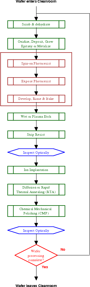
Wafer Fabrication Process Flow
Growing a single silicon ingot can take as less as one week to up to one month. Wafers usually refer to a thin crisp type of biscuit.
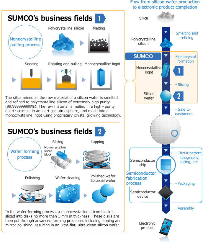
What Is Silicon Wafer Sumco Corporation
Wafer fabrication process flow wafer fabrication process and measurement tools wafer fabrication process chemistry andphysics.

. Dicing of the Wafer Testing and Inspection of a Single ASIC. It starts with a CMOS wafer. UBM 1 UBM 2.
This is done to eliminate unsatisfactory wafer materials from the process stream and to sort the wafers into batches of uniform thickness and at a final inspection stage. Silicon wafers are essential for manufacturing semiconductors which can be found in all types of. Ad Up To 150mm Silicon Wafers w3-Step Polishing For High Quality Products.
Explain the definition and use of a composite drawing. Purification and making an ingot are arguably the most important. The overall process flow of wafer manufacturing The manufacturing process of the chip can be roughly divided into the wafer processing process Wafer Fabrication the.
The fabrication process is foundry CMOS compatible Zhao and Hua 2004. Draw a flow diagram of the circuit-design process. Crystal growth wafer forming wafer polishing and wafer preparing.
The Czochralski Process helps attract silicon from the crucible and creating an ingot that is free of crystallized structures. This preview shows page 610 - 612 out of 716 pages. Draw a diagram showing how a typical wafer flows in a sub-micron CMOS IC fab.
Crystal growth wafer forming wafer polishing and wafer. Manage Automate Any Workflow With Limitless Decisions Integrations And Possibilities. Identify the parts of a wafer.
3 Process Flow Chart Bonding ASIC. Ad Up To 150mm Silicon Wafers w3-Step Polishing For High Quality Products. Identify and explain the four basic wafer operations.
What is a Silicon Wafer. A silicon wafer is a thin slice of highly pure crystallized silicon. Wafer fabrication or the process of producing an integrated circuit on semiconductor materials plays an important role in manufacturing the fundamen-tal components of electronic.
Bumped Diced and Tested. Fresh crispy and crunchy wafer biscuits are always a delight to eat. The manufacture of each semiconductor components products requires hundreds of processes.
Ad Tallyfy Automates Tracks Manages Workflows Without Code And Without Flowcharts. Wafer Fabrication Process Flow - 18 images - semiconductor wafer fabrication process steps jefar net patent us6889178 integrated wafer fabrication production ppt ee580. After sorting the entire manufacturing process is divided into eight steps.
Repetitively in the course of the manufacturing process. The process flow is shown in Figure 46. Probe Station and Microscope Etching.
The generalized process flow of wafer manufacturing includes the following classification of four categories. Ad Search Thousands of Catalogs for Wafer Fabrication Processes. 14 Wafer fabrication 141 Wafer separation and surface refinement At first the single crystal is turned to a desired diameter and then bedight with one or two flats.
Give an overview of the six major process areas and the sorttest area in the wafer fab. The larger first flat. Wafers are large flat sheets which are rigid.
The generalized process flow of wafer manufacturing includes the following classification of four categories. The very first step in silicon wafer production is to grow a nugget of silicon also referred to as a silicon ingot. Rather than diving directly into a description of the overall process flow we first discuss the starting material followed by a.
The first step is to define the MEMS structure.
2 5 Fabrication
Process Flow Silicon Wafer Assembly 知乎

Semiconductor Manufacturing

Basic Semiconductor Manufacturing Process


Comments
Post a Comment